
Tô Châu Shengyifurui Công ty TNHH Công nghệ Điện tử
008613771901136
 Tiếng Việt
Tô Châu Shengyifurui Công ty TNHH Công nghệ Điện tử
Tiếng Việt

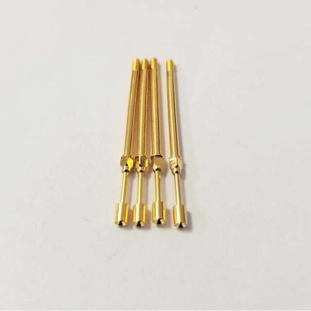
A test probe is a tool commonly used in electronic testing and measurement, and gold plating is a common surface treatment used to improve the probe's conductivity and corrosion resistance. However, the thickness range of test probe gold plating is not fixed and depends on the specific application and needs.
Generally speaking, the thickness of gold plating on test probes can range from a few microns to tens of microns. (short test pin probe supplier china) Thinner gold plating layers are usually between 1-5 microns, while thicker gold plating layers can reach 10-30 microns. The choice of this range depends on several factors, including the purpose of the probe, the requirements of the test environment, and budget constraints.
Thinner gold plating layers are suitable for some precision electronic test and measurement applications, such as microelectronic chip testing, semiconductor device testing, etc. This is because a thin gold plating layer can provide good conductivity without having too much impact on the object being measured. In addition, a thinner gold plating layer can also reduce the resistance and contact resistance between the test probe and the object being measured, improving the accuracy and reliability of the test.
However, in some special applications, a thicker gold plating layer is required to provide better corrosion resistance and long-term stability. (5a Current Coaxial Probe Test Probe) For example, in some harsh test environments, such as high temperature, high humidity, corrosive gas, etc., a thicker gold plating layer can provide better protection and extend the service life of the test probe.
It should be noted that the thickness of the gold plating of the test probe is not as thick as possible. An excessively thick gold plating layer may increase the stiffness of the probe, affecting its sensitivity and adaptability. In addition, an excessively thick gold plating layer may increase costs and manufacturing difficulties.
Therefore, when selecting the thickness of gold plating for test probes, multiple factors need to be considered and weighed based on specific applications and needs. The optimal thickness range should be to minimize the impact on the object being measured on the basis of meeting the requirements of conductivity, corrosion resistance and cost.


 English